Novel technologies to advance next-generation semiconductor packaging
Precise and high-speed bonding onto a 300 mm waffle wafer for a new power distribution channel that enables high-quality power delivery
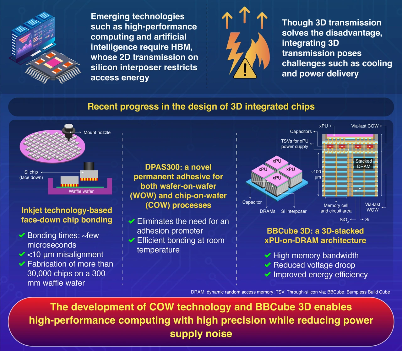
A novel power supply technology for 3D-integrated chips has been developed by employing a three-dimensionally stacked computing architecture consisting of processing units placed directly above stacks of dynamic random access memory. Towards realizing this, researchers developed key technologies involving precise and high-speed bonding technique and adhesive technology. These new technologies can help in addressing the demands of high-performance computing applications, which require both high memory bandwidth and low power consumption with reduced power supply noise.
Advancements in the Design and Development of 3D Computing Architectures
Advanced Resin Material Enabling Room-Temperature Bonding for WOW and COW 3DI Applications
BBCube 3D: Fully Vertical Heterogeneous Integration of DRAMs and xPUs Using a New Power Distribution Highway
Chujo et al. (2025) | 2025 IEEE 75th Electronic Components and Technology Conference (ECTC)
From simple household appliances like televisions to laptops and smartwatches, electronic devices have transformed our everyday lives. Advancements in semiconductor fabrication technologies and chip packaging processes have been central to the explosive growth of these electronic devices. However, in today’s age of artificial intelligence (AI) and high-performance computing, the need for faster processors with enhanced power efficiencies remains unmet.
Traditional system-in-package (SiP) approaches, where semiconductor chips are arranged in a two-dimensional plane (2D) using solder bumps, have size-related limitations, warranting the development of novel chip integration technologies. In this light, a team of researchers from Institute of Science Tokyo (Science Tokyo), Japan, has conceptualized an innovative 2.5D/3D chip integration approach called BBCubeTM. Furthermore, to drive the practical realization of BBCubeTM, they have developed three key technologies. Their research findings and outcomes were recently presented at the 2025 IEEE 75th Electronic Components and Technology Conference (ECTC), held from May 27 to May 30, 2025.
The research team, comprising Specially Appointed Professors Norio Chujo, Takayuki Ohba and other scientists from the Institute of Integrated Research’s WOW Alliance Heterogeneous and Functional Integration Unit at Institute of Science Tokyo (Science Tokyo), Japan, initially developed a face-down chip-on-wafer (COW) process to circumvent the limitations of using solder interconnects. Utilizing inkjet technology and a selective adhesive coating method, they successfully carried out sequential bonding of different chip sizes onto a 300 mm waffle wafer with a narrow chip-to-chip spacing of 10 μm and a minimal mount loading time of less than 10 milliseconds. Explaining the precise COW process, Chujo comments, “More than 30,000 chips of various sizes were fabricated onto the waffle wafer, achieving enhanced bonding speed without any chip-detachment failures.”
To enable this precise and high-speed COW process, the researchers turned their attention to addressing thermal stability issues that can affect multilevel stacking of ultra-thin wafers. By carefully designing the chemical properties, they developed a novel adhesive material that can be used in both COW and wafer-on-wafer processes called ‘DPAS300.’ This new adhesive, composed of an organic–inorganic hybrid structure, exhibited appreciable adhesiveness and heat resistance during experimental studies.
Finally, to achieve high memory bandwidth and improve the power integrity of BBCubeTM, the scientists employed a 3D xPU-on-DRAM architecture reinforced by a new power distribution highway. This included embedding capacitors between xPU and DRAM, implementing redistribution layers on the waffle wafer, and placing through-silicon vias in wafer lanes and DRAM scribe lines. “These innovations reduced the energy required for data transmission to one-fifth to one-twentieth of that in conventional systems, while also suppressing power supply noise to below 50 mV,” states Chujo, highlighting the benefits of 3D stacked computing architecture.
Taken together, the chip integration technologies developed by researchers from Science Tokyo have the potential to transform next-generation computing architectures.
These novel technologies have been published under the titles “Face-Down Bonding and Heterogeneous Chiplet Integration by Using Bumpless Chip-on-Wafer (COW) with Waffle Wafer Technology,” “Advanced Resin Material Enabling Room-Temperature Bonding for WOW and COW 3DI Applications,” and “BBCube 3D: Fully Vertical Heterogeneous Integration of DRAMs and xPUs Using a New Power Distribution Highway.”
Reference
- Journal:
- Proceedings of the 2025 IEEE 75th Electronic Components and Technology Conference (ECTC)
- Authors:
- Yoshiaki Satake1, Wataru Doi1, Hajime Kato1, Shogo Okita1, Tatsuya Funaki1, and Takayuki Ohba1
- Title:
- Face-Down Bonding and Heterogeneous Chiplet Integration by Using Bumpless Chip-on-Wafer (COW) with Waffle Wafer Technology
- Authors:
- Naoko Araki1, Tadashi Fukuda1, and Takayuki Ohba1
- Title:
- Advanced Resin Material Enabling Room-Temperature Bonding for WOW and COW 3DI Applications
- Authors:
- Norio Chujo1*, Hiroyuki Ryoson1, Koji Sakui1, Shinji Sugatani1, Masao Taguchi1, and Takayuki Ohba1
- Title:
- BBCube 3D: Fully Vertical Heterogeneous Integration of DRAMs and xPUs Using a New Power Distribution Highway
- Affiliations:
- 1WOW alliance, Institute of Science Tokyo, Japan
Related articles
Further Information
Specially Appointed Professor Norio Chujo
Heterogeneous and Functional Integration Unit, The WOW Alliance, Institute of Integrated Research
Contact
Public Relations Division, Institute of Science Tokyo
- media@adm.isct.ac.jp
- Tel
- +81-3-5734-2975