New nanogap architecture enables electrically driven narrow-line-width emission in monolayer WSe2
Researchers have developed a new planar device architecture that can achieve electrically driven narrow-line-width light emission
A monolayer tungsten diselenide-based planar architecture featuring curved gold/platinum electrodes separated by a gap of less than 5 nm can produce narrow-line-width alternating-current electroluminescence, show researchers. The curved nanogap topography is expected to generate a nonuniform nanoscale strain landscape, which may influence the local electronic environment. The proposed device offers reproducible narrow-line-width emission, without requiring precise stacking of 2D materials, making it a promising architecture for on-chip quantum light sources suitable for quantum photonic devices.
Narrow-Line-Width Localized Emission in 2D Materials
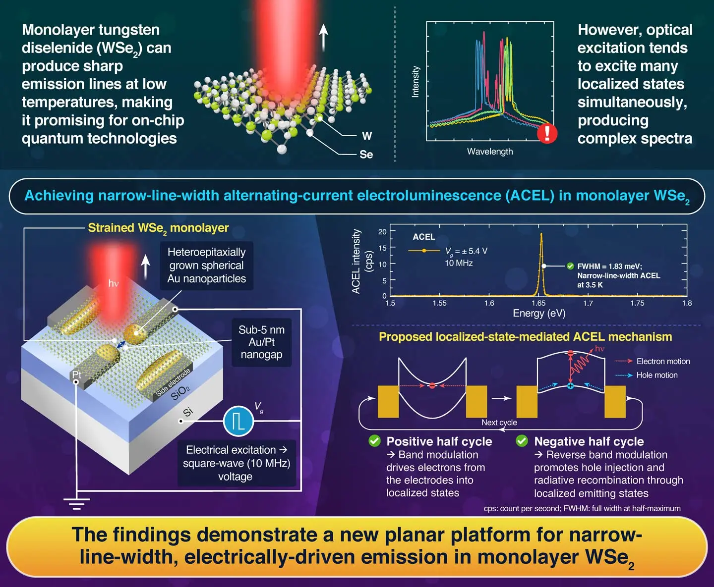
Quantum light sources that emit light with special quantum properties, such as single photons, are critical for quantum photonic technologies, including quantum communication, computing, and sensing. In this regard, monolayer tungsten diselenide (WSe2), a two-dimensional (2D) semiconductor material, hosts localized emissive states that enable light emission with sharp or narrow-line-widths, meaning that the emitted light has a narrow range of photon energies. This sharp luminescence makes this material a promising candidate for implementing on-chip quantum light sources.
However, its potential for on-chip integration is hindered by fundamental limitations of optical excitation technologies. Conventional optical excitation approaches tend to excite multiple localized states simultaneously, producing light emission with a complex spectrum containing multiple peaks. In addition, reliance on an external laser complicates on-chip integration. On the other hand, electrical excitation approaches can address this issue, but many existing devices rely on precise stacking of multiple 2D materials, involving complex fabrication processes that limit scalability and yield.
Addressing these challenges, an international research team led by Professor Yutaka Majima from the Materials and Structures Laboratory at Institute of Science Tokyo (Science Tokyo), Japan, and Professor Ali Javey of the University of California, USA, have now developed a fully on-chip nanogap platform that generates narrow-line-width alternating-current electroluminescence (ACEL) from the monolayer WSe2. Their study was made available online on October 03, 2026, and published in Volume 26, Issue 40 of the journal Nano Letters on October 14, 2026.
“Our approach integrates monolayer WSe2 with heteroepitaxial gold/platinum (Au/Pt) electrodes separated by a gap of less than 5 nm,” explains Majima. “This structure achieves electrically driven narrow-line-width emission without requiring precise 2D material stacking.”
The Au/Pt electrodes, with a gap less than 5 nm wide, were fabricated using electron-beam lithography and electroless gold plating. The monolayer WSe2 was then dry-transferred onto the prepatterned electrodes.
By applying a 10 MHz square-wave voltage to the silicon back gate while grounding both Au/Pt nanogap electrodes, the researchers observed ACEL at 3.5 K with an apparent fitted line width of 1.83 meV. In contrast, under optical excitation the same device produced light emission with a broad, complex spectrum with multiple peaks. This difference indicates that electrical excitation through the sub-5 nm nanogap preferentially accesses a smaller subset of localized states near the junction, which can be selectively accessed through electrical excitation. The narrow-line-width ACEL could be reproduced consistently across multiple such devices.
To investigate the mechanism behind this behaviour, the team conducted electric-field simulations and structural analyses. The findings suggest that the curved nanogap electrodes produce a highly nonuniform nanoscale strain distribution in the monolayer WSe2, which may modify the local electronic environment. Electrostatic simulations also show regions of enhanced electric field near the curved Au/WSe2 contact boundaries, potentially contributing to the selective electrical excitation of localized states. Analysis of the ACEL spectra also supported a localized-state emission. The researchers also found that this localized-state-mediated ACEL mechanism was promoted by the rapid voltage transitions of the square-wave AC excitation, which drive phase-dependent carrier injection and recombination.
To evaluate the reproducibility of the narrow-line-width electroluminescence behavior, the researchers analyzed 49 devices, of which 15 exhibited narrow-line-width ACEL. Statistical evaluation of these devices, together with separate control experiments using wider electrode gaps or insulating spacers and measurements under different excitation conditions, indicated that the narrow-gap geometry, enhanced local electric field, and rapid voltage transitions are important for producing narrow-line-width ACEL.
“Our findings demonstrate a new platform for narrow-line-width, electrically driven localized emission in 2D materials,” remarks Javey. “More broadly, the scalable, planar architecture of the device will be highly beneficial for developing nanoscale quantum light sources that are suitable for on-chip integration, supporting integrated quantum photonic devices.”
Overall, this study offers a new nanogap architecture for developing planar quantum light sources with narrow-line widths.
Reference
- Authors:
- Shurong Miao1,2,3, I. K. M. Reaz Rahman2,3, Aditya Nirmale1, Inha Kim2,3, Dorottya Urmossy2,3, Thomas P. Darlington4, Harishankar Jayakumar4, Seiichiro Izawa1, Archana Raja4,5, Daryl C. Chrzan3,6, Yutaka Majima2,* and Ali Javey1,3,5*
*Corresponding authors - Title:
- Narrow-Line-Width Electroluminescence in Monolayer WSe2 Enabled by a Sub-5 nm Au/Pt Nanogap
- Journal:
- Nano Letters 26, 13862–13870, 2026.
- Affiliations:
- 1Electrical Engineering and Computer Sciences, University of California, Berkeley, USA
2Materials and Structures Laboratory, Institute of Science Tokyo, Japan
3Materials Sciences Division, Lawrence Berkeley National Laboratory, USA
4The Molecular Foundry, Lawrence Berkeley National Laboratory, USA
5Kavli Energy NanoScience Institute, University of California, Berkeley, USA
6Department of Materials Science and Engineering, University of California, Berkeley, USA
Related articles
Further information
Professor Yutaka Majima
Institute of Integrated research, Institute of Science Tokyo
Contact
Public Relations Division, Institute of Science Tokyo
- media@adm.isct.ac.jp
- Tel
- +81-3-5734-2975